Plus Two Physics Chapter Wise Previous Questions Chapter 14 Semiconductor Electronics: Materials, Devices and Simple Circuits is part of Kerala Plus Two Physics Chapter Wise Previous Questions and Answers Kerala. Here we have given Plus Two Physics Chapter Wise Questions and Answers Chapter 14 Semiconductor Electronics: Materials, Devices and Simple Circuits.
Kerala Plus Two Physics Chapter Wise Previous Questions Chapter 14 Semiconductor Electronics: Materials, Devices and Simple Circuits
Question 1.
The band gap at 300K of crystals A, B, C, D is 5.5, 1.2, 0.67 and 0.1 units respectively. Answer the following questions based on this information. (March – 2009)
a) What do you understand by band gap?
b) What is the most common unit to measure band gap?
c) In the above case, which crystal will have the highest electrical conductivity at 300K? Why?
Answer:
a) The energy difference between the conduction . band and valency band is called band gap or forbidden gap.
b) Electron volt (ev)
c) Crystal D. Because it has least band gap energy.
Question 2.
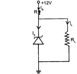
Considers zenerdiode with the breakdown voltage 6.2V (March – 2009)
a) How is zener diode different from an ordinary diode?
b) What is the significance of the breakdown voltage for a zener diode?
c) Write any one application of zener diode
d) What is the voltage drop across the resistor R in the circuit shown below? The zener diode has a breakdown voltage of 6.2V.
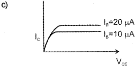
p) Consider the following circuit diagram of a transistor:
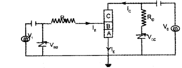
Which type of transistor is used in the circuit? How did you identify?
q) Which application of the transistor is shown in the circuit diagram?
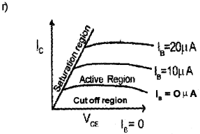
r) Sketch the output characteristics of a transistor in the CE configuration. Mark the saturation region, cut off region and active region in the characteristics curve.
Answer:
a) Zener is heavily doped compared to ordinary diode (or) Zener diode is used in reverse bias whereas ordinary diode works in forwarding bias.
b) It is the constant voltage across zener diode in reverse bias at which the current increases rapidly.
c) Voltage Regulator
d) V = VR + Vz, VR = V – Vz, V = 12V, Vz = 6.2V
∴ V = 5.8V
OR
p) npn, The direction of current flow shows that this is npn transistor.
q) Amplifier
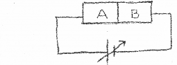
Question 3.
A student made a circuit as shown in the figure, S1 and S2 are switches and B is a bulb. (March – 2010)
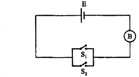
a) He argues that this circuit is equivalent to an AND gate. Do you agree with him? Justify your answer.
b) Write down its truth table.
Answer:
a) The working of the circuit can be written as
| s1 | s2 | Bulb |
| OFF | ON | ON |
| ON | OFF | ON |
| OFF | OFF | OFF |
| ON | ON | ON |
The above working shows that the circuit is OR gate
b) Truth table
| A | B | c |
| 0 | 1 | 1 |
| 1 | 0 | 1 |
| 0 | 0 | 0 |
| 1 | 1 | 1 |
Question 4.
A photodiode is fabricated from a semiconductor of band gap energy 2.8 eV. (March – 2010)
a) Define band gap.
b) Can this photodiode be used to detect a wavelength of 500nm? Justify your answer.
Answer:
a) The valence band and the conduction band are separated by an energy gap. This energy gap is called band gap.
b) The energy of 5 nm,
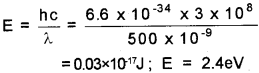
The energy of incident wave is 2.4eV. But the band gap is 2.8eV. Hence no photocurrent is pro-duced due to the incident wave of energy 2.4eV. Hence this diode can’t used to detect a wave of wavelength 500nm.
Question 5.
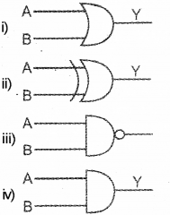
For the logic circuit shown below, with inputs ‘a’ and ‘b’ and output ‘x’. (Say – 2010)
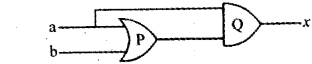
a) Identify the logic gates marked P & Q.
b) Write down the output 1×1, when a = 1, b = O and a = O, b = 1.
Answer:
a) P – OR gate
Q – AND gate
b)
| a | b | X |
| 1 | 0 | 1 |
| 0 | 1 | 0 |
Question 6.
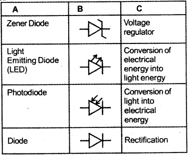
Match the following in 3 columns. (March – 2011)
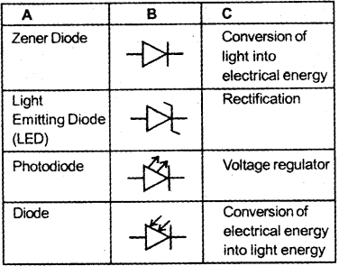
Answer:
Question 7.
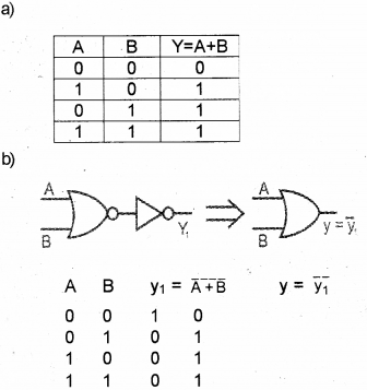
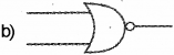
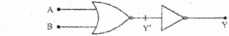
Consider the logic circuit using NOR gates given below: (March – 2011)
![]()
a) Write the truth table for the circuit.
b) Identify the logic operation which this circuit is performing.
Answer:
| A | B | Y |
| 1 | 0 | 1 |
| 0 | 1 | 1 |
| 1 | 1 | 1 |
| 0 | 0 | 0 |
b) Or gate
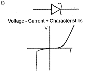
Question 8.
As you know diodes are inevitable components of electronic circuits to meet the specific requirements of our daily life. (March – 2011)
a) Name the diode which regulates the output of an unregulated supply.
b) Draw its circuits symbol and general shape of its volt-ampere (V-l) characteristics.
Answer:
a) Zener diode
Question 9.
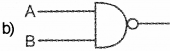
Given below is the truth table of a 2-input logic gate. (March – 2012)
| A | B | Output |
| 0 | 0 | 1 |
| 0 | 1 | 1 |
| 1 | 0 | 0 |
| 1 | 1 | 0 |
a) Identify the logic gate.
b) Draw its logic symbol.
c) If this logic gate is connected to a NOT gate, what will be the output, when
i) A = 1, B = 1 and
ii) A = 0, B = 1?
Answer:
There ¡s mistake in question.
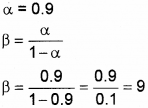
Question 10.
a) Choose the correct relation between the transistor parameters α and β. (March – 2012)
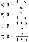
b) Define the quantities α and β.
c) Give their possible range of values.
Answer:
![]()
b) The ratio of collector current to emitter current in common base configuration is α. The ratio of collector current to base current in common emitter configuration is β.
c) α = 0.9 ______ 0.99
β = 20 ______ 200
Question 1.
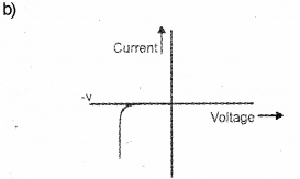
A p-n junction has various applications as in diode, transistor etc. A p-n junction with a bias voltage is shown below. (March – 2012)
a) Comment on the current flow across the junction under this condition.
b) Howa zener diode is different from an ordinary p-n junction diode?
c) Draw the reverse characteristics of a zener diode and an ordinary p-n junction diode.
d) With a diagram explain the action of a zener diode as a voltage regulator.
Answer:
a) This diode is kept at reverse bias. Hense current through diode is very small.
b) Zener diode is heavly dopped. It is designed to operate under reverse bias. The depletion region of zener is very thin.
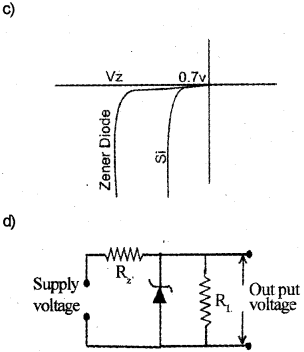
The zener diode is connected to a fluctuating voilage supply through a resistor Rz. The out put is taken across RL.
Working
When ever the supply voltage increases beyond the break down voltage, the current through zener increases (and also through Rz). Thus the voltage across Rz increases, by keeping the voltage drop across zener diode as a constant value. (This voltage drop across Rz is proportional to the input voltage)
Similaiy, when supply voltage decreases beyond a certain value, the current through the zenerdi ode decreases. Thus the voltage across Rz de-creases, by keeping the voltage drop across zener diode as constant (Zener diode as a voltage regulator)
Question 11.
The oscillator is a circuit that generates signals of desired frequencies and an amplifier is used to amplify the signals. (March – 2012)
a) Why positive feedback is applied in an oscillator?
b) When transister is used as an amplifier, common emitter configuration is used. Why?
c) Draw a circuit diagram common-emitter charac teristics. Draw output characteristics for two in put current.
Answer:
a) Positive feedback is used to keep energy of LC oscillation as constant (un damaped).
b) A common emitter transistor amplifier is preferred when we require better current gain and power gain.
Question 12.
Biasing is provided for maintaining proper current flow across a p-n junction. (March-2013)
a) In a biased p-n junction the net flow of holes is from ‘n’ region to ‘p’ region.
b) For the device shown below draw the V -1 characteristics when the potential is applied between the terminals A and B.
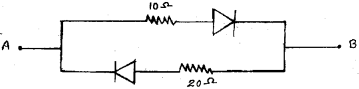
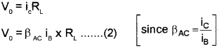
c) A transistor can be used to amplify voltage or current. Explain how a transistor can be used as a current amplifier. Draw necessary circuit.
Answer:
a) Reverse biased
b) When we apply a dc voltage across A and B we get V – I graph as shown below.
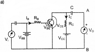
Working:
Case 1: When there is no input signal (ie. V1 = O,)
The input voltage can be written as VBa = VBE + IB RB
This base voltage produces a base current IB With in turn produces a dc collector current IC. The output voltage can be written as VCE = VCC – lC RC
This dc output voltage is unable to produce an out put signal due to the presence of a capacitor. Be cause, the capacitor prevents the flow of dc current through it.
Case 2 : When there is an input ac signal, (ie. V1 ≠ O)
when we apply an AC signal as input, we get an AC base current denoted by i. Hence input AC voltage can be written as
VB = îBr …..(1)
where ‘r’ is the effective input resistance.
ThisAC input current produces anAC output current (ic) which can flow through a capacitor. Hence the output voltage can be written as VB = iC x output resistance. If we take output resistance as RL then V0 becomes
Question 13.
Two semiconductor materials A and B shown in the given figure are made by doping germanium crysal with arsenic and indium respectively. The two are joined end to end and connected to a battery as shown. (Say – 2013)
a) Will the junction be forward biased or reverse bi-ased? Justify your answer.
b) Sketch a V-l graph for his arrangement.
Answer:
a) Reverse biased
The region A is n-type and B is P-type.
Question 14.
A gate allows the signals to pass through only when some logical conditions are satisfied. (Say – 2013)
a) Write the truth table of ‘OR’ gate.
b) The output of a 2-input LNORI gate is fed to a ‘NOT’ gate. Draw the logic circuit of this combi nation of gates and write the truth table for the output of the combination for all inputs.
Answer:
Question 15.
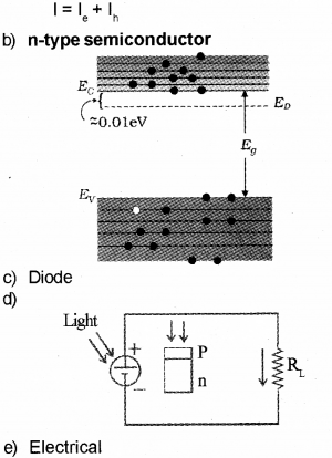
We are familiar $#h the semi conductors Silicon and Germanium. (March – 2014)
a) With a necessary schematic diagram, briefly explain the characteristics of an intrinsic semiconductor.
b) Drawthe energy bands of a n-type semiconductor.
c) The following figure represents a
d) Draw a typical illuminated P-n junction solar cell.
e) LED convert energy to light.
Answer:
a) A semiconductor in its pure form is called intrinsic semiconductor.
1) In intrinsic semiconductor the number of free electrons is equal to number of holes.
2) The total current in intrinsic semi conductor is the sum of free electron current I and hole current lh.
Question 16.
You are given two p-n junction diodes.
a) Mention the name of an electronic circuit which make use of these diodes to convert A.C. current to continuous D.C. current. (Say – 2014)
b) Draw the circuit diagram of the above mentioned circuit.
Answer:
a) Rectifier
b) Refer Q.P. March 2015, Q.No. (OR) 2 (B)
Question 17.
The truth table of a logic circuit is given below:
| A | B | Y |
| 0 | 0 | 1 |
| 0 | 1 | 1 |
| 1 | 0 | 1 |
| 1 | 1 | 0 |
a) Identify the gate.
b) Which of the following isthe logic symbol of this gate?
Answer:
a) NAND
Question 18.
The truth table of a logic gate is given below.: (March – 2015)
| A | B | Y |
| 0 | 0 | 1 |
| 0 | 1 | 0 |
| 1 | 0 | 0 |
| 1 | 1 | 0 |
a) Identify the gate.
b) Draw the logic symbol of the gate.
c) Explain why NAND gate is known as universal gate.
Answer:
a) NOR gate
c) All gates can be constructed using NAND gate. Hence NAND gate is known as universal gate.
Question 19.
[The following is a choice question. Answer any one.] (March – 2015)
a) Draw the circuit diagram of transistor as an am plifier in common emitter configuration.
b) Obtain the expression for the voltage gain.
OR
a) What do you mean by berner potential of a diode?
b) With the helpof a diagram explain the working of a full wave rectifier.
Answer:
b) When we apply an AC signal as input, we get an AC base current denoted by iB. Hence input AC voltage can be written as
V1 = iBr ………………….. (1)
where ‘r is the effective input resistance.
ThisAC input current produces an AC output current (iC) which can flow through a capacitor.
Hence the output voltage can be written as V0 = iC x output resistance. If we take output resistance as RL then V0 be comes
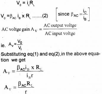
Power gain
The power gain A can be expressed as the product of the current gain and voltage gain. ie. power gain Ap = βac x A
OR
A) Barrier Potential
The n-region losses electrons and p-region gains electrons. Because of this a potential is developed across the junction and it tends to prevent movement of electron from n-side to p-side. This potential is called barrier potential.
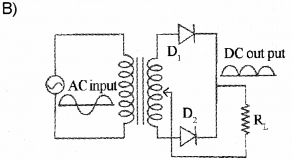
Full wave rectifier consists of tía nsforrner. two diodes and a load resistance RL. Input a.c signal is applied across the primary of the transformer. Seconclary of the transformer is connected to D1 and D2. The output is taken across RL.
Working
During the +ve half cycle of the a.c signal at secondary, the diode D1 is forward biased and D2 is reverse biased. So that current flows through D1 and RL.
During the negative half cycle of the a.c signal at secondary, the diode D1 is reverse biased and D2 is forward biased. So that current flows through D2 and RL. Thus during both the half cycles, the current flows through RL in the same direction. Thus we get a +ve voltage across RL for +ve and -ve input. This process is called full wave rectification.
Question 20.
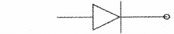
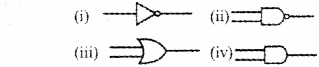
a) Which of the following symbol represents a universal gate? (March – 2016)
b) Shown below is an experimental set up with a semiconductor diode
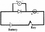
i) identify the experiment
ii) draw the resulting graph
c) With the help of neat circuit diagram obtain an expression for voltage gain of a transistor amplifier in C-E configuration.
Answer:
![]()
b) i) this experiment is to study forward character istics of pn junction diode (V-I graph).
c) Refer Qn.No. 2B March -2015
Question 21.
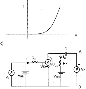
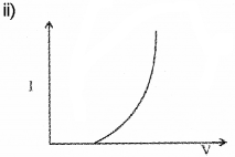
A graph showing the vañation of current (I) flow ng through a p-n junction wfth the voltage (V) applied across it is called the V-l characteristic of a p-n junction. (Say – 2016)
a) V-l characteristic of a forward biased diode is shown in the figure.
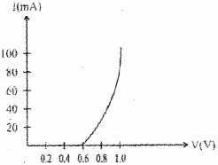
Write any two important features of the graph.
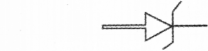
b) What is a zener diode? Give its symbol.
Answer:
a) The resistance of diode is low in forward bias. The current increases rapidly with voltage after a particular value of bias voltage. This voltage is
called bias voltage.
b) Zenerdiode isa heavily doped p-n junction diode that works in reverse bias. The symbol is
Question 22.
A logic circuit is shown in the figure: (Say – 2016)
Complete the truth table of the circuit:
| A | B | Y’ | Y |
| 0 | 0 | 1 | 0 |
Name the resulting gate formed by the combination of the above gates.
Answer:
| A | B | Y | Y |
| 0 | 0 | 1 | 0 |
| 1 | 0 | 0 | 1 |
| 0 | 1 | 0 | 1 |
| 1 | 1 | 0 | 1 |
Question 23.
A Zener diode is always operated in bias. (March – 2017)
Answer:
Reverse
Question 2.
Write down the truth table of a NOR gate.
Answer:
Question 24.
The current amplification factor for CB configuration of a transistor is 0.9. Find out the current amplification factor for CE configuration. (March – 2017)
Answer:
Question 25.
Which of the following relation is correct for a transistor? (Say – 2017)
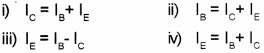
Answer:
![]()
Question 26.
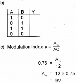
A network of logic gates is shown in the figure. (Say – 2017)
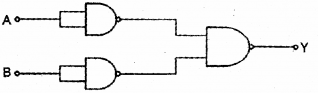
a) Identify the gates used in this circuit.
b) Write the truth table of this combination of gates.
c) A carrier wave of peak voltage 12 Volt is used to transmit a message signal. Find the peak value of the voltage of the modulating signal in order to have a modulation index of 75%.
Answer:
a) NAND gate
We hope the Kerala Plus Two Chemistry Chapter Wise Questions and Answers Chapter 14 Semiconductor Electronics: Materials, Devices and Simple Circuits help you. If you have any query regarding Kerala Plus Two Chemistry Chapter Wise Questions and Answers Chapter 14 Semiconductor Electronics: Materials, Devices and Simple Circuits, drop a comment below and we will get back to you at the earliest