Plus Two Physics Notes Chapter 14 Semiconductor Electronics: Materials, Devices and Simple Circuits is part of Plus Two Physics Notes. Here we have given Plus Two Physics Notes Chapter 14 Semiconductor Electronics: Materials, Devices and Simple Circuits.
| Board | SCERT, Kerala |
| Text Book | NCERT Based |
| Class | Plus Two |
| Subject | Physics Notes |
| Chapter | Chapter 14 |
| Chapter Name | Semiconductor Electronics: Materials, Devices and Simple Circuits |
| Category | Plus Two Kerala |
Kerala Plus Two Physics Notes Chapter 14 Semiconductor Electronics: Materials, Devices and Simple Circuits
Introduction
Before the discovery of transistor, vacuum tube or valves were considered as the building blocks of electronic circuit.
1. A Comparison of Vacuum Tubes and Transistors:
| Vacuum Tubes/valves | Transistors |
| 1. External heating is required. (Electrons are supplied by heated cathode) | No external heating is required. |
| 2. Large evacuated space (vacuum) is required be tween cathode and anode | Evacuated space is not required |
| 3. The electrons from heated cathode flows through vacuum. | The charge carriers flows within solid itself. |
| 4. Bulky (large in size) | Small in size |
| 5. Consume high power | Low power consumption |
| 6. Operate at high voltage | Operate at low voltage |
| 7. Limited life arid low reliability. | Long life and high reliability. |
Classification Of Metals, Conductors, And Semiconductors
1. On the basis of conductivity:
On the basis of relative values of electrical conductivity (σ) and resistivity ρ = \(\frac{1}{\sigma}\) solids are classified as
(i) Metals:
They possess very low resistivity (or high conductivity).
ρ → 10-2 – 10-8 Ω m
σ → 102 – 108 S m-1
(ii) Semiconductor:
They have resistivity or conductivity intermediate to metals and insulators.
ρ → 10-5 – 106 Ω m
σ → 105 – 10-6 S m-1
(iii) Insulators: They have high resistivity (or low conductivity).
ρ → 1011 – 1019 Ω m
σ → 10-11 – 10-19 S m-1
2. Band Theory: Conduction Band, Valence Band, and Energy Gap:
In an isolated atom, electrons will have definite energy level. When atoms combine to form solid, the energy levels of outer electrons overlap. Hence outer energy levels split in to many energy levels.
These energy levels are very closely spaced Hence it appears as continuous variation of energy. This collection of energy levels are called energy band.
The energy band which includes energy levels of valence electrons is called valence band. The energy band above valence band which includes energy levels of conduction electrons is called conduction band.
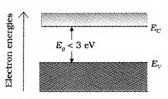
The gap between the top of valence band and bottom of conduction band is called energy band gap (Energy gap, Eg).
Energy level diagram of different bands:

The band gap energy of Ge and Si are 0.3ev and 0.7ev respectively.
3. Classification on the basis of Energy bands Conductors:
Conduction band is partially filled and valence band is partially empty.
OR
Conduction band and valence band are overlapped so that Eg = 0ev

Due to overlapping, electrons are partially filled in conduction band. These partially filled electrons are responsible for current conduction.
Insulators:
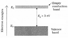
Conduction band is empty. Valence band may fully or partially filled. There is a wide energy gap between valence band and conduction band (Eg > 3ev).
Semiconductors:
Conduction band may be empty or lightly filled. Valence band is fully filled. The energy gap is very small (< 3ev)
At room temperature some electrons in valence band get enough energy to cross the energy gap and move into conduction. Hence semiconductors show intermediate conductivity.
Intrinsic Semiconductor
A semiconductor in its pure form is called intrinsic semiconductor.
For intrinsic semiconductor:
* The number of free electrons is equal to number of holes.
ie. ne = nh = ni
ne, nh and ni are the free electron concentration, hole concentration and intrinsic carrier concentration.
Explanation:
Each Si atom is covalently bonded to nearest four neighboring atoms. When temperature increase, some of covalent bond brakes and electrons become free leaving a vacancy (hole). Thus each free electron creates hole in the lattice. Hence number of free electrons equals number of holes.
* The total current in intrinsic semi conductor is the sum of free electron current Ie and hole current Ih.
I = Ie + Ih
Explanation:
When an electric field is applied, free electrons move towards positive potential and give rise to electron current, le. The holes move towards negative potential and give rise to hole current. Thus total current is contributed by both free electrons and holes.
Extrinsic Semiconductor
1. Extrinsic semiconductor or impurity semiconductor:
The addition of suitable impurity improves the conductivity of intrinsic semiconductors. Such semiconductors are called extrinsic semiconductor. They are of two types n-type and p-type semiconductors.
2. Doping and Dopants:
The deliberate addition of suitable impurity to semiconductors to improve its conductivity is called doping.
The impurity atoms are called dopants. There are two types of dopants;
- Pentavalent (valency 5): Arsenic (As), Antimony (Sb), Bismuth (Bi), Phosphorous (P), etc.
- Trivalent (Valency 3): Indium (In), Boron (B), Aluminium (Al), etc.
3. n-type semiconductor:
When a pentavalent impurity is added to Si crystal, four electrons of impurity atom make bond with neighboring four Si atoms. The fifth electron remains weakly bound to its parent atom.
At room temperature this electron become free to move. Thus each pentavalent atom donate one extra electron for conduction and hence it is called donor impurity.
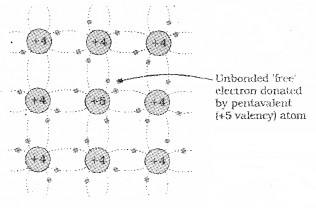
Thus in doped semiconductor the number of conduction electrons will be large compared to number of holes. Hence electrons are the majority carriers and holes the minority carriers. Hence semiconductors doped with pentavalent impurity is called n-type semiconductor.
Note:
In n-type semiconductors
ne >> nh
But as a whole n-type semiconductor is neutral (ie. electrons is equal and opposite to ionized (donor) core in lattice).
4. p-type semiconductor:
When a trivalent impurity is added to Si crystal, three electrons of impurity atom make covalent bond with neighboring three Si atom. The fourth bond with neighboring Si atom lacks one electron. Thus a vacancy or a hole is created in fourth bond.
The neighboring Si atom needs an electron to fill the vacancy and hence one electron in outer orbit of nearby Si atom move to this vacancy leaving a hole in its own site. Thus hole can move through the lattice.
Each trivalent atom creates a hole and it act as acceptor. Hence it is called acceptor impurity. The semiconductor doped with trivalent impurity has more number of holes than free electrons. Here holes are the majority carriers and electrons are the minority carriers. Hence it is called p-type semiconductor.
Note: I
(I) In p-type semi conductor
nh >> ne
But as a whole p-type semiconductor is electrically neutral. (The charge of additional holes is equal and opposite to acceptor ions).
(II) In thermal equilibrium electron and hole concentration in a semiconductor is given by nenh = n2r.
5. Energy band structure of Extrinsic semiconductors
n-type semiconductor:
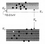
In n-type semiconductors, the donor energy level (ED) is slightly below conduction band.
P-type semiconductor:

In p-type semiconductors, the acceptor energy level (EA) lies slightly above valence bond.
p-n Junction
A p-n junction is basic building block of semiconductor devices like diode, transistor, etc.
1. p-n junction formation:
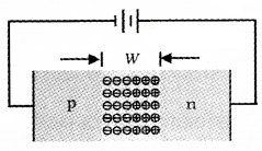
When pentavalent impurity is added to a part of p-type Si semiconductor wafer, we get both p region and n region in a single wafer.
The formation of p-n junction includes two processes.
(i) Diffusion:
In n type semiconductor, concentration of electrons is more than that of holes. In p-region, the hole concentration is more than electron concentration. Because of this concentration gradient, electrons diffuse from n side to p-side and holes diffuse from p-side to n-side during the formation of p-n junction. This produces diffusion current.
(ii) Drifting – Formation of Depletion region:
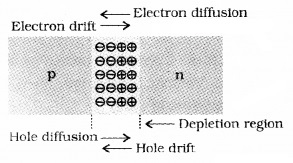
When electrons diffuses from n to p, it leaves behind positively charged immobile donor ions on n-side. As electrons continue to diffuse from n to p, a layer of positive charge is developed on n- side.
Similarly when holes diffuse from p to n, it leaves behind negatively charged immobile ions on p side. As holes continue to diffuse from p to n, negative space charge region is developed on p side.
The positive space-charge region on n-side and negative space-charge region on p-side, is known as depletion region. This region contain only immobile ions.
2. Barrier Potential:
The n-region losses electrons and p-region gains electrons. Because of this a potential is developed across the junction. This potential is called barrier potential.
Semiconductor Diodes
A semiconductor diode is a p-n junction provided with metallic contact at both ends to apply external voltage.
The symbol of p-n junction diode is given below.
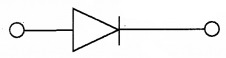
The arrow shows conventional direction of current.
1. p-n junction diode under forward bias:
When p-side of p-n junction diode is connected to positive terminal of the battery and n-side to the negative terminal it is said to be in forward biased.

Due to the applied voltage, electrons of n-side get repelled by negative terminal of battery. Hence they cross depletion region and reach at p-side.
similarly the holes of p-side get repelled by positive terminal of battery and cross depletion region, reach n-side. The total forward current is sum of hole current and current due to electron.
2. p-n junction diode under reverse bias:
When p-side of p-n junction diode is connected to negative terminal of battery and n-side to the positive terminal, it is said to be in reversed biased.
In reverse bias the electrons of n-side and holes on p-side cannot cross the junction. But the minority carriers – holes on n-side and electrons on p-side drift across the junction and produce current. The reverse current is of the order micro ampere.
Note: Junction width increases in reverse bias.
Breakdown Voltage (VBr):
The reverse current remains independent of bias voltage up to a critical reverse bias voltage called reverse break down voltage. At breakdown voltage, reverse current increases sharply.
V-I characteristics:
To study variation of current with voltage for p-n junction diode, it is connected to a battery through a rheostat. Rheostat is used to vary the biasing voltage. A milliammeter is connected in series with diode to study forward current.
To measure reverse current microammeter is used. A voltmeter is connected across diode to measure voltage. The current is measured for different values of volt and a graph (V-I) is plotted.

In forward bias, current first increases very slowly up to a certain value of bias voltage. After this voltage, diode current increases rapidly. This voltage is called Knee voltage or cut-in voltage or threshold voltage. (0.2v for Ge and 0.7v for Si). The diode offers low resistance in forward bias.
In reverse bias, current is very small. It remains almost constant up to break down voltage (called reverse saturation current). Afterthis voltage reverse current increases sharply.
Note:
(i) In forward bias, resistance is low compared to reverse bias.
(ii) The dynamic resistance of diode is defined as ratio of change in voltage to change in current.
rd = \(\frac{\Delta v}{\Delta l}\)
Application Of Junction Diode
Diode as a rectifier:
The process of converting AC into DC is known as Rectification. A p-n junction diode conducts current when it is forward biased, and does not conduct when it is reverse biased. This feature of the junction diode enables it to be used as rectifier.
1. Diode as half wave rectifier:
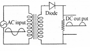
Circuit details:
A half wave rectifier consists of transformer, a diode and a load resistor RL. The primary coil of transformer is connected to a.c input and secondary is connected to RL through diode.
Working:
During the positive half cycle of the input a.c at secondary, the diode is forward biased and hence it conducts through RL. During negative half cycle of a.c at secondary, diode is reverse biased and does not conduct. Thus, we get +ve half cycle at the output. Hence the a.c input is converted into d.c output.
2. Full wave rectifier:
Circuit details:
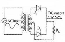
Full wave rectifier consists of transformer, two diodes, and a load resistance RL. Input a.c signal is applied across the primary of the transformer. Secondary of the transformer is connected to D1 and D2. The output is taken across RL.
Working:
During the +ve half cycle of the a.c signal at secondary, the diode D1 is forward biased and D2 is reverse biased. So that current flows through D1 and RL.
During the negative half cycle of the a.c signal at secondary, the diode D1 is reverse biased and D2 is forward biased. So that current flows through D2 and RL.
Thus during both the half-cycles, the current flows through RL in the same direction. Thus we get a +ve voltage across RL for +ve and -ve input. This process is called full-wave rectification.
Special Purpose p-n Junction Diodes
1. Zener diode:
Zener diode is designed to operate under reverse bias in the breakdown region. It is used as a voltage regulator. The symbol for Zener diode is shown in figure.

Zener diode is heavily dopped. Hence depletion region is very thin.
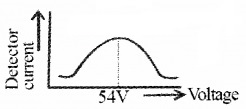
I-V characteristics of zener diode:
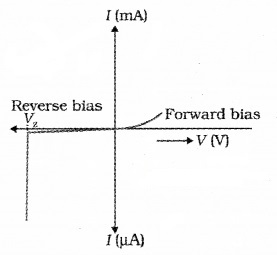
The l-V characteristics of a Zener diode is shown in above figure. At break down voltage, current increases rapidly. After breakdown, zener voltage remains constant. This property of the Zenerdiode is used for regulating supply voltages.
Explanation for large reverse current:
Reverse current is due to the flow of electrons (minority carriers) from p to n and holes from n to p. When the reverse bias voltage increases and becomes V = V2 high electric field is developed. This high electric field can pull valence electrons from the atoms. These electrons account for high current.
1. (a) Zener diode as avoltage regulator Principle:
In reverse breakdown region, the voltage across the diode remains constant.
Circuit details:
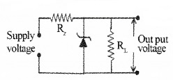
The Zener diode is connected to a fluctuating voltage supply through a resistor Rz. The output is taken across RL.
Working:
Whenever the supply voltage increases beyond the breakdown voltage, the current through zener increases (and also through Rz).
Thus the voltage across Rz increases, by keeping the voltage drop across zenerdiode as a constant value. (This voltage drop across Rz is proportional to the input voltage).
2. Optoelectronic junction devices:
(i) Photodiode:
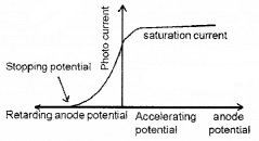
The photodiode can be used as a photodetector to detect optical signals.
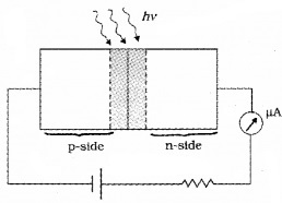
It is operated under reverse bias. When the photodiode is illuminated with light (photons) electron-hole pairs are generated. Due to electric field of the junction, electrons and holes are separated before they recombine.
The direction of the electric field is such that electrons reach n-side and holes reach p-side. Electrons collected on n-side and holes collected on p- side produce an emf. When an external load is connected, the current flows through the load.
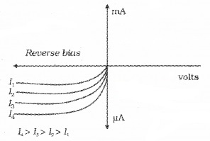
The I-V characteristics of a photodiode:
(ii) Light-emitting diode [LED]:
LED is heavily doped pn junction diode working under forward bias .Gallium Arsenide is used for making infrared LEDs.
Working:
When the junction diode is forward biased, electrons and holes flow in opposite directions across junction. Some of the electrons and holes combine at junction and energy is produced in the form of light.
Uses:
LEDs are used in remote controls, burglar alarm systems, optical communication, etc.
Advantages of LED over conventional incandescent lamps:
- Low operational voltage and less power.
- Fast action and no warm-up time required.
- The bandwidth of emitted light is 100 A° to 500 A° or in other words it is nearly (but not exactly) monochromatic.
- Long life and ruggedness.
- Fast on-off switching capability.
3. Solar cell:
Solar cell is junction diode used to convert solar energy into electrical energy.
Circuit details:
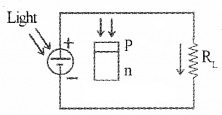
Its p-region is thin and transparent and is called emitter. The n-region is thick and is called base. Output is taken across RL.
Working:
When light falls on this layer, electrons from the n-region cross to the p-region and holes in the p-region cross in to the n-region. Thus a voltage is developed across RL. Solar cells are used to charge storage batteries during daytime.
The I-V characteristics of a solar cell:
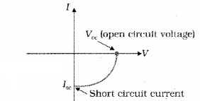
The I-V characteristics of solar cell is drawn in the fourth quadrant of the coordinate axes. This is because a solar cell does not draw current but supplies the same to the load.
Junction Transistor
1. Transistor: structure and action
Transistor is a three-layered doped semiconductor device. There are two types of transistors:
- n-p-n transistor
- p-n-p transistor.
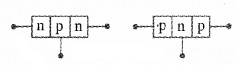
Symbols:

Naming the transistor terminals:
A transistor has 3 terminals:
- Emitter
- Collector
- Base.
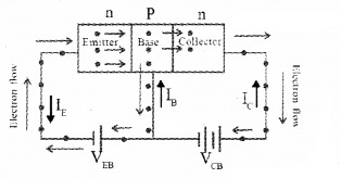
1. Emitter:
The section, which supplies charge carriers, is called emitter. Emitter is heavily doped. The emitter should be forward biased.
2. Collector:
The section which collects the charge carriers, is called collector. Collector is moderately doped. The collector should be reverse biased.
3. Base:
Middle section between emitter and ‘ collector is called base. Base is lightly doped.
Transistor action:
Circuit details:
Emitter is maintained at forward bias and collector is maintained at reverse bias. VEB is the emitter base voltage and VCB is the collector base voltage.
Working:
Emitter is kept at forward bias so that the electrons are ejected into base. Thus an emitter current IE is produced.
At the base, electron-hole combination takes place. As the base is lightly doped and very thin, only a few electrons combine with holes to constitute the base current, IB.
The remaining electrons are attracted towards collector because the collector is kept at reverse bias. Due to this electron flow, a collector current IC is produced.
In this way, the emitter current is divided into base current and collector current.
Mathematically this can be written as
IE = IB + IC
IB > is small, so IE = IC
2. Basic transistor circuit configurations and transistor characteristics:
Transistor can be used in three modes:
- Common base configuration
- Common emitter configuration
- Common collector configuration
a. Common base configuration:

In Common base configuration .base is common to both input and output
Current amplification = \(\frac{\text { output current }}{\text { input current }}\)
Current amplification, α = \(\frac{l_{C}}{l_{E}}\)
b. Common emitter configuration:

Current amplification = \(\frac{\text { output current }}{\text { input current }}\)
Current amplification, β = \(\frac{l_{C}}{l_{B}}\)
c. Common collector configuration:
Current amplification γ = \(\frac{l_{E}}{l_{B}}\)
Relation between α and β:
i.e. β = \(\frac{\alpha}{I-\alpha}\)
Common Emitter Configuration:

Input Characteristics (CE configuration):
The graph connecting base current with base-emitter voltage (at constant VCE) is the input characteristics of the transistor.

To study the input characteristics, the collector to emitter voltage (VCE) is kept at constant. The base current IB against VBE is plotted in a graph.
The ratio ∆ VBE/∆ IB at constant VCE is called the input resistance.
i.e,,Input resistance \(r_{1}=\frac{\Delta V_{B E}}{\Delta I_{B}}\)
Output Characteristics (CE. Configuration):
The output characteristics is a graph connecting the collector current lc with collector-emitter voltage (VCE) at a constant base current (IB).
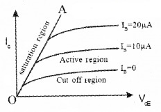
This is obtained by measuring the collector current IB at different collector voltage by keeping the base current fixed.
Line OA is called saturation line .The region right of the saturation line is the active region. Transistor is operated as amplifier in this region. The region below IB = 0 is the cut off region.
The output resistance is the ratio of a small change in collector voltage to the change in collector current at constant base current.
Output resistance \(\mathrm{r}_{0}=\frac{\Delta \mathrm{V}_{\mathrm{CE}}}{\Delta \mathrm{I}_{\mathrm{C}}}\)
3. Transistor as a device
Transistor as a switch:
A circuit diagram for transistor switch is given below.
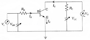
Applying Kirchoff’s voltage rule to the input side of this circuit, we get
VBB = IBRB + VBE
and applying Kirchoff’s voltage rule to the output side of this circuit, we get
VCE = VCC – ICRC.
We shall treat VBB as the dc input voltage Vi and VCE as the dc output voltage Vo.
So, we have
Vi = IBRB + VBE ____(1) and
Vo = VCC – ICRi______(2)
The variation of output voltage with input voltage:
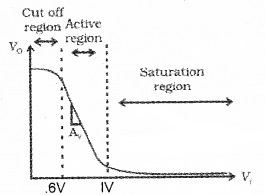
The variation of output voltage with input voltage is shown in the above graph. This graph contain three regions
- cut off region
- Active region
- saturation region.
a. Cut off region:
In the case of Si transistor, if input voltage Vi is less than 0.6V, the transistor will be in cut off state and out put current (Ic) will be zero.
Substituting Ic = 0 in the eq (2) we get out put voltage Vo = VCC
b. Active region:
When Vi becomes greater than 0.6 V the transistor is in active state with some current Ic. The eq(2) shows that, the output Vo decrease as the term IcRc increases. With increase of Vi, Ic increases almost linearly and so Vo decreases linearly till its value becomes less than about 1.0 V.
Note:
Amplifier is working in the active region.
c. saturation region:
When the output voltage becomes 1.0V, the change becomes non linear and transistor goes into saturation state. With further increase in Vi the output voltage is found to decrease towards zero (though it may never become zero).
Working of transistor as switch:
When Vi is low (unable to give forward-bias to the transistor) we get high output (ie. Vo = Vcc). In this stage the transistor doesn’t conduct. Hence transistor is said to be switched off.
If Vi is high enough to drive the transistor into saturation, then Vo is low (very near to zero). In this stage the transistor driven into saturation it is said to be switched on.
Note:
The switching circuits are designed in such a way that the transistor does not remain in active state.
4. Transistoras an Amplifier (CE-Configuration):
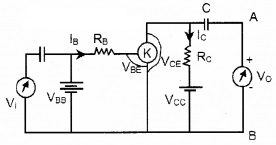
The working of an amplifier can be explained using the circuit given above. It is an n-p-n transistor connected in common emitter configuration. VBB is the biasing voltage used in the input side and Vcc is the reverse bias voltage used in the output side.
RB is the resistor connected to base in order to reduce the base current. Rc is the resistor which is connected in between Vcc and collector terminal. We take the voltage across Rc and Vcc with the help of a capacitor C. We maintain voltages VBB and Vcc such that the transistor is always on the active region.
Working:
Case 1:
When there is no input signal (ie. Vi = 0,)
The input voltage can be written as
VBB = VBE + IBRB
This base voltage produces a base current IB which in turn produces a dc collector current IC. The output voltage can be written as
VCE = VCC – ICRC
This dc output voltage is unable to produce an output signal due to the presence of a capacitor. Because, the capacitor prevents the flow of dc current through it.
Case 2:
When there is an input ac signal, (ie. Vi ≠ 0):
when we apply an AC signal as input, we get an AC base current denoted by iB. Hence input AC voltage can be written as
Vi = iBr ______(1)
where ‘r’ is the effective input resistance.
This AC input current produces an AC output current (ic) which can flow through a capacitor. Hence the output voltage can be written as
V0 = ic × output resistance
If we take output resistance as RL then vo becomes
V0 = ic RL
V0 = βAC ic × RL _____(2) [since βAC = \(\frac{\mathrm{i}_{\mathrm{C}}}{\mathrm{i}_{\mathrm{B}}}\)]

Power gain:
The power gain Apcan be expressed as the product of the current gain and voltage gain.
ie. power gain Aρ = βac × Av
Note:
The transistor is not a power generating device. The energy for the higher ac power at the output is supplied by the battery.
5. Feedback amplifier and transistor oscillator 9.13 Oscillator:
A transistor amplifier can be converted into an oscillator by positive feedback, (positive feedback means that a small portion of the output signal is applied to the input in-phase).
Circuit Details:
The battery Vcc is connected in between C (collector) and E (emitter) through a coil L1. Another coil Lis connected in between B (base) and E. A capacitor is connected in parallel to coil L.
Working:
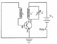

When the key is pressed a small current flows through the coil L11. The variation of current in the coil L1 produces a change in flux. This change in flux induces a voltage across L.
As a result, the forward voltage increases which further increases the emitter and collector current. This again increases the forward voltage. This process continues till the collector gets saturated.
When the collector current is saturated (constant), the flux also becomes steady and the induced emf becomes zero. This reduces collector current. The decrease in collector current induces a voltage in L in the opposite direction (reverse voltage). As a result the collector current decreases further.
This continues until the collector current falls below its normal value. After this, the collector current build up and the process is repeated. Thus oscillation of frequency.
f = \(\frac{1}{2 \pi \sqrt{L C}}\) is produced.
Digital Electronics And Logic Gates
In digital electronics, we use two levels of voltage (represented by 0 and 1). Such signals are called digital signals. Logic gates are the building blocks of digital circuits. Logic gates are used in calculators, digital watches, computers, robots, industrial control systems, and in telecommunication.
1. Logic gates:
A logic gate is a digital circuit that follows certain logical relationship between input and output voltage. Hence it is so called. The funda¬mental logic gates are AND, OR, NOT, NAND, and NOR. The truth table gives all possible input logic level combinations with their respective output logic levels.
(i) NOT gate:
The most basic gate which has only a single input and single output. It is also called inverter. It produces an inverted version of input. The Boolean expression is y = \(\overline{\mathrm{A}}\)
The symbol is

A The truth table is
| Input | Output |
| A | Y |
| 1 | 0 |
| 0 | 1 |
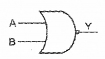
(ii) OR gate:
It has two or more inputs but a single output. The output is high when either inputs or both inputs are high.
The Boolean expression is Y = A + B (read as A or B)
The symbol is
![]()
The truth table:

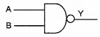
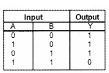
(iii) AND gate:
It has two or more inputs but a single output. The output is high only if both inputs are high. The Boolean express of output is Y = A.B (read as A and B)
The symbol is

The truth table

(iv) NAND gate (or bubbled AND gate):
This is an AND gate followed by NOT gate. The Boolean expression is y = \(\overline{\mathrm{A.B}}\)
The symbol is
The truth table
(v) NOR gate (or bubbled OR gate):
It has two or more inputs and one output. This is OR gate followed by NOT gate.
The Boolean expression is Y = \(\overline{A+B}\)
The symbol is
The truth table is

NAND gate and NOR gate are called universal gates because other basic gates like OR, AND and NOT gate can be realized using them.
Integrated Circuits
The entire circuit fabricated on a small piece of semiconductor or chip is called Integrated Circuit (IC). It contains many transistors, diodes, resistors, capacitors, connecting wires – all in one package.
It was invented by Jack Kilky in 1958 and won Nobel prize for this invention. IC’s are produced by a process called photolithography. IC’s are categorized depending on nature of input signals.
(a) Linear or analogue IC:
These IC’s handle analogue signals and output varies linearly with input.
Eg: Operational Amplifier
(b) The digital IC:
These type handles digital signals and mainly contain logic gates Depending on the level of integration (number of circuit components or logic gates), IC are classified as
- SSI – Small scale Integration (logic gates ≤ 10)
- MSI – Medium Scale Integration (logic gates ≤ 100))
- LSI – Large scale Integration (logic gates ≤ 1000)
- VLSI – Very Large scale integration (logic gates > 1000)
The miniaturization in electronics technology is brought about by the Integrated circuit. It has made the things faster and smaller. IC is the heart of computer system. In fact IC’s are found in almost all electrical devices like cars, televisions, CD players, cell phones, etc.
We hope the Plus Two Physics Notes Chapter 14 Semiconductor Electronics: Materials, Devices and Simple Circuits help you. If you have any query regarding Plus Two Physics Notes Chapter 14 Semiconductor Electronics: Materials, Devices and Simple Circuits, drop a comment below and we will get back to you at the earliest.