Understanding Semiconductor Diodes
Semiconductors: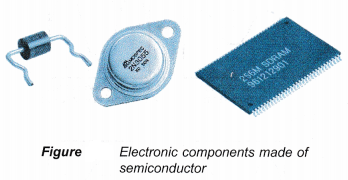
- Figure shows the various types of electronic components made of semiconductor materials.
- A semiconductor is a material which can conduct electricity better than insulators, but not as well as conductors.
- The conductivity of a material can be explained in terms of its resistance and free electrons.
- Metals are good conductors of electricity because they have many free electrons that can move easily between atoms. The resistance of metals is generally very low.
- Insulators are poor conductors of electricity because they have too few free electrons to move about to conduct electricity. Therefore, insulators have very high resistance.
- A semiconductor behaves as an insulator at very low temperature, with appreciable electrical conductivity at room temperature although it is still much lower than a conductor.
- Semiconductors can be pure elements, such as silicon or germanium, or compounds such as gallium arsenide or cadmium selenide.
- In a process called doping, small amounts of impurities are added to pure semiconductors causing large changes in the conductivity of the material.
People also ask
- What do you mean by rectification?
- What is a half wave rectifier?
- What do you mean by logic gates?
- What is meant by combinational logic circuits?
- How does a transistor works as an amplifier?
- How can a transistor be used as a switch?
Properties of a Semiconductor
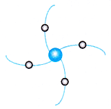
- Examples of typical semiconductor materials are silicon and germanium. They have a unique property in their electron structure. Each has four electrons in its outer orbital as shown in Figure.
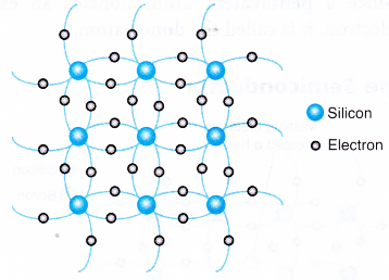
- Figure shows the outer electrons in a silicon crystal. All the electrons are involved in perfect covalent bonds, leaving no free electrons to conduct electricity.
- At very low temperatures, pure silicon crystal is nearly an insulator and has a high resistance to current flow. However, as the temperature of pure silicon crystal increases, some electrons gain sufficient energy to break free.
- Figure shows the electrons and holes in a semiconductor.
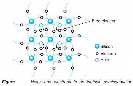
- For every electron that is free, there is a hole in the bonding structure between the atoms of the crystal. Since the atoms are neutral when they have a complete set of electrons, the hole behaves as if it has a positive charge.
- Like the free electrons, these positive holes seem to move through the semiconductor material and form part of the electric current in it.
- In semiconductors, the current flow is facilitated by both the electrons and holes. Therefore, electrons and holes are known as the charge carriers in a semiconductor.
- An intrinsic semiconductor is made of pure materials such as silicon or germanium. It derives its semiconductor properties from its own atoms only and hence, it is called an intrinsic semiconductor. When a potential difference is applied across an intrinsic semiconductor, it conducts a very small current.
- The charge carriers are thermally created by excited electrons jumping from the valence band into the conduction band.
- Thus, the charge carriers are equally divided where the number of free electrons present in an intrinsic semiconductor is the same as the number of holes.
- When an intrinsic semiconductor is connected in a circuit as shown in Figure, the current which flows in it consists of both electron current and hole current. However, the electron current and hole current are not necessarily equal due to their different effective masses.
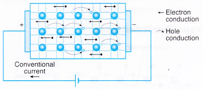
- The free electrons, which have been freed from their lattice positions, can move through the conduction band. In addition, other electrons can hop between lattice positions to fill the vacancies left by the freed electrons.
- This additional mechanism is called hole conduction because it is as if the holes are migrating across the conduction band in the direction opposite to the free electron movement.
- The concentration of charge carriers in an intrinsic semiconductor is greatly affected by temperature.
Importance of Doping in Semiconductors
- Doping is a process of adding a certain amount of specific impurities, called dopants, to a semiconductor material to increase its conductivity.
- A small amount of dopants can change the electronic properties of semiconductors in a controllable way.
- An extrinsic semiconductor is a semiconductor that has a certain amount of impurities added to it. For example, a tiny amount of gallium or arsenic is added to silicon to increase its conductivity. We can say that the silicon has been doped with gallium or arsenic. Adding such impurities to silicon modifies the number and type of free charge carriers.
- Doping process produces two groups of semiconductors. They are the n-type (negative charge conductor) and p-type (positive charge conductor) semiconductors.
n-type Semiconductor: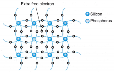
- n-type doping increases the number of free electrons in a doped semiconductor.
- As an intrinsic semiconductor, a silicon atom has four valence electrons. Each of these electrons is shared with each of the neighbouring silicon atoms to form a covalent bond.
- If atoms with five valence electrons (pentavalent atoms), such as phosphorus (P), arsenic (As), or antimony (Sb), are doped into the intrinsic semiconductor to replace some of the silicon atoms, then each of the pentavalent atoms will have four covalent bonds and one extra electron. These pentavalent atoms produce the n-type semiconductor by contributing extra electrons.
- These extra electrons are weakly bound to the atoms and are free to move about. As a result, there are more free electrons than holes.
- In this case, the electrons are the majority carriers and the holes are the minority carriers.
- Since a pentavalent atom donates an extra electron, it is called the donor atom.
p-type Semiconductor: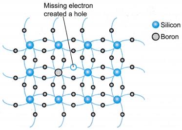
- p-type doping increases the number of holes in a doped semiconductor.
- In the case of silicon, if atoms with three Valence electrons (trivalent atoms) such as boron, aluminium, indium or gallium are doped into the intrinsic semiconductor to replace some of the silicon atoms, then the result is that one electron is missing from one of the four covalent bonds. These trivalent atoms produce the p-type semiconductor by creating deficiencies of valence electrons called holes.
- A dopant atom replaces the missing electron by accepting the electron from the covalent bond of a neighbouring atom to complete the bond.
- When the dopant atom accepts the electron from its neighbouring atom, a hole is created in the neighbouring atom instead.
- If more trivalent atoms are added into the semiconductor, there will be more holes than free electrons.
- In this case, the holes are the majority carriers and the free electrons are the minority carriers.
- Since a trivalent atom accepts an electron, it is called the acceptor atom.
Semiconductor Diodes
- A semiconductor diode is a device made from a p-n junction.
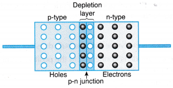
- A p-n junction is formed when pieces of n-type and p-type semiconductors are fused together.
- At the junction of a p-type and an n-type semiconductors, a region called the depletion layer is formed.
- At the depletion layer, some free electrons from the n-type diffuse across the junction into the p-type and fill up the holes. The holes from the p-type appear to move across the junction to the n-type.
- The nature of the depletion layer is that it will block the current flow from the n-type region to the p-type region, but will allow the current to flow from the p-type region to the n-type region.
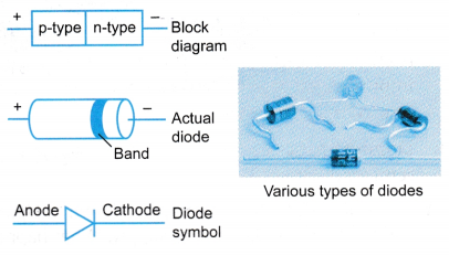
- When two electrodes are attached to the two ends of a p-n junction, it is called a diode.
- A diode is a device that allows current to flow in one direction only but blocks it in the opposite direction. It is more like an electronic check device.
How does the diode work?
- There are two ways a diode can be connected in series to a battery, in forward bias or reverse bias.
- In forward bias, the p-type (anode) of the diode is connected to the positive terminal and the n-type (cathode) is connected to the negative terminal of a battery as shown in Figure.
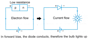
- The holes from the p-type material and the electrons from the n-type material are pushed to the p-n junction. At the junction, the electrons and holes combine to ensure a continuous current flow. Therefore, the bulb lights up.
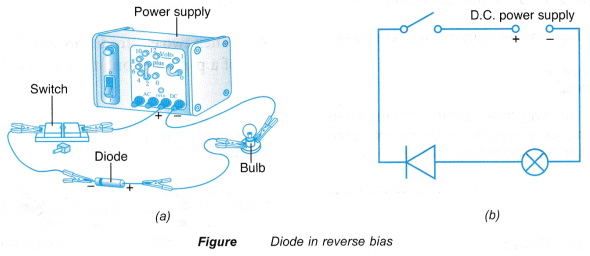
- In reverse bias, the n-type is connected to the positive terminal and the p-type is connected to the negative terminal of the battery as shown in Figure.
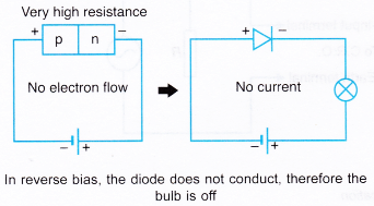
- The reversed polarity causes a very small current to flow as both electrons and holes are pulled away from the junction.
- When the potential difference due to the widened depletion layer equals the voltage of the battery, the current will cease except for the small thermal current. Therefore, the bulb does not light up.
- Diodes have a low resistance when they are forward-biased and a very high resistance when they are reverse-biased.
- Figure shows the I-V characteristic graph for an ideal diode.
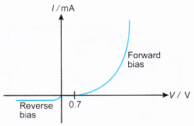
- When forward-biased, there is a small amount of voltage necessary to conduct the diode. In silicon, this voltage is about 0.7 V before the current climbs to an appreciable level. This voltage is needed to start the hole-electron combination process at the junction.
- When reverse-biased, only a small current of 10 mA will pass through the diode. However, in the case of an ideal diode, there is no current flowing through the diode.
Semiconductor Diode in Forward Bias or Reverse Bias Experiment
Aim: To observe current flow through a semiconductor diode in forward bias or reverse bias.
Materials: Diode, bulb, switch, connecting wires
Apparatus: D.C. power supply
Method:
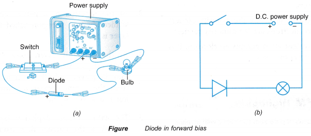
- The electrical circuit is set up as shown in Figure. The cathode of the diode is connected to the negative terminal of the d.c. power supply. What happens to the bulb is observed.
- The connection of the diode is reversed as shown in Figure. The cathode of the diode is connected to the positive terminal of the d.c. power supply. What happens to the bulb is observed.
Discussion:
- When the diode is in forward bias, the bulb lights up. When the diode is in reverse bias, the bulb does not light up.
- The current will flow when the diode is in forward bias where the anode is connected to the positive terminal and the cathode is connected to the negative terminal of the power supply.
- The function of a diode is to allow current to pass through in one direction only.