What do you mean by logic gates?
- A logic gate is a switching circuit that is applied in computers and other electronic devices.
- It is the basic electronic building block used in computers and many other digital devices.
- A logic gate performs logical operation in a digital system.
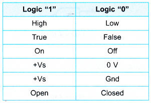
- A digital system is where the input and output only involve two levels of voltage, high (1) or low (0).
- Table shows the other names for the logic levels.
- The logic gates are called ‘gates’ because they give a ‘1’ on the output only when a particular combination of 0 and 1 is present at the inputs. This combination is the ‘key’ to open the gate which is the output.
Logic Gates as Switching Circuits
- A logic gate is a switching circuit made up of a combination of transistor switches.
- It has one or more input terminals but only one output terminal.
- It is useful to find out how some simple logic gates can be built from switches. A closed switch is considered to be at a high state (1) and an open switch is at a low state (0).
- Switches in series can perform an AND gate function and switches in parallel can perform an OR gate function.
Symbols for Logic Gates
- A logic gate can be represented by a block diagram as shown in Figure.
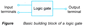
- In practice, each logic gate is represented by a symbol with input terminals and one output terminal.
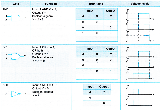
- The three basic logic gates are called AND, OR and NOT gates.
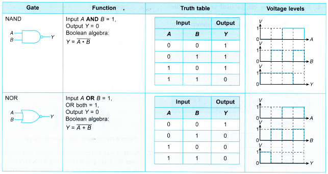
- A NAND gate is made of an AND gate and a NOT gate, while a NOR gate is made of an OR gate and a NOT gate.
- At any given moment, a terminal of a logic gate is in one of the two states, low (0) or high (1), represented by different voltage levels.
- The voltage at the output terminal or state depends on the voltages or states at the input terminals. This means that each logic gate only ‘opens’ and gives a ‘high’ output for certain input combinations.
People also ask
- What is meant by combinational logic circuits?
- Understanding Semiconductor Diodes
- What do you mean by rectification?
- How does a transistor works as an amplifier?
- How can a transistor be used as a switch?
AND Gate
- Figure shows the circuit diagram for AND gate.
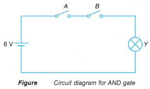
- When switches A and B are open, the logic state is 0. When switches A and B are closed the logic state is 1.
- When the bulb does not light up, the logic state is 0. When the bulb lights up, the logic state is 1.
- Switch A and switch B represent the inputs while bulb Y represents the output.
- Bulb Y will only light up if both switch A AND switch B are closed.
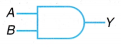
- Figure shows the symbol for AND gate.
OR Gate
- Figure shows the circuit diagram for OR gate.
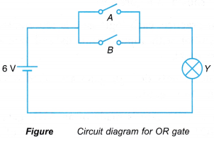
- Bulb Y will light up when switch A OR switch B (or both) are closed. Otherwise, the bulb does not light up.
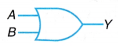
- Figure shows the symbol for OR gate.
NOT Gate
- Figure shows the circuit diagram for NOT gate.
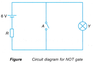
- Bulb Y will light up if switch A is open but will NOT light up if switch A is closed.
- Figure shows the symbol for NOT gate. A NOT gate can only have one input and one output.
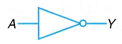
- A NOT gate is also called an inverter.
NAND Gate
- Figure shows the circuit diagram for NAND.
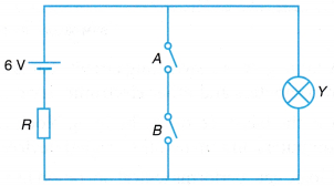
- Bulb Y will NOT light up if both switch A AND switch B are closed.
- Figure shows the symbol for NAND gate.
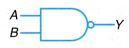
- A NAND gate is an AND gate combined with a NOT gate. Therefore, a NAND gate is the NOT of an AND gate.
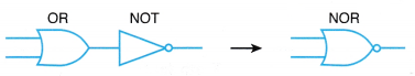
NOR Gate
- Figure shows the circuit diagram for NOR gate.
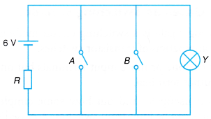
- Bulb Y will NOT light up if switch A OR switch B (or both) are closed.
- Figure shows the symbol for NOR gate.
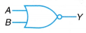
- A NOR gate is an OR gate combined with a NOT gate as in Figure. Therefore a NOR gate is the NOT of an OR gate.
Truth Tables for Logic Gates
- A truth table is used to record all the possible combinations of inputs and the corresponding output decisions for a particular logic circuit.
- The behaviour of the logic circuit can be summarised by a truth table.
- In a truth table, the input and output states are represented by the binary numbers 0 (low) and 1 (high).
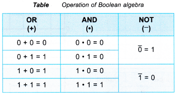
- Boolean algebra can be used tp descrihe the switching functions of logic gates. The operation of the Boolean algebra can be shown as in Table.
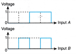
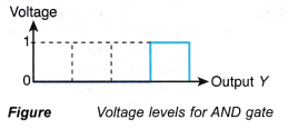
- The voltage levels (low or high) can be used to represent the inputs and output states of a logic gate.
- Figure shows an example of inputs and output voltages of an AND gate.
- Another way to represent the inputs and output states of a logic gate is by writing the binary states on the terminals of the logic gate as shown in Figure.
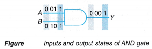
Table summarises the action of the five basic logic gates.
Logic Gates Experiment
Aim: To study the actions of AND, OR, NOT, NAND and NOR gates
Material: Connecting wires
Apparatus: Circuit modules for AND, OR, NOT, NAND and NOR gates, a.c. power supply
Method: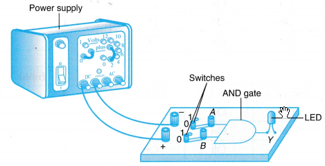
- The apparatus is set up as shown in Figure.
- The activities as in Table are carried out for the AND, OR, NOT, NAND and NOR circuit modules.
- The observations are recorded.
Observations:
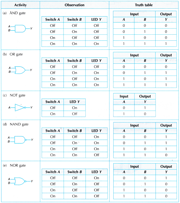
Discussion:
- The NOT gate is called an inverter because its output is the inverse of its input.
- The NAND gate is an AND gate with the output inverted. It is the NOT of an AND gate.
- The NOR gate is an OR gate with the output inverted. It is the NOT of an OR gate.